


Arts Festival weekend attracts alumni and family back to State College
With one daughter a Penn State alumna, another daughter a current student, and their son a hopeful Nittany Lion, the Stoffas have instilled in their family what Penn State has instilled in them—pride. They’ll return to Happy Valley this summer to express that pride during Arts Festival Weekend 2017, taking place July 12–16.
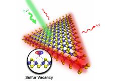
A fast, non-destructive test for two-dimensional materials
Thinning a material down to a single-atom thickness can dramatically change that material's physical properties. For example, graphene, the best-known 2D material, has unparalleled strength and electrical conductivity, unlike its bulk form, graphite. Researchers have begun to study hundreds of other 2D materials for the purposes of electronics, sensing, early cancer diagnosis, water desalination and a host of other applications. Now, a team of Penn State researchers in the Department of Physics and the Center for Two-Dimensional and Layered Materials (2DLM) has developed a fast, nondestructive optical method for analyzing defects in 2D materials.
Outstanding faculty and students honored at annual College of EMS awards banquet
The possibilities for the new field of two-dimensional, one-atomic-layer-thick materials, including but not limited to graphene, appear almost limitless. In new research, Penn State material scientists report two discoveries that will provide a simple and effective way to "stencil" high-quality 2D materials in precise locations and overcome a barrier to their use in next-generation electronics.

Penn State opens mapping course on FutureLearn MOOC platform
Penn State’s massive open online course “Maps and the Geospatial Revolution” will open May 8 on FutureLearn, the United Kingdom’s leading MOOC platform.
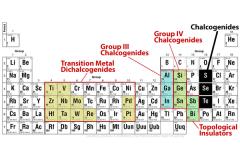
Stenciling with atoms in two-dimensional materials possible
The possibilities for the new field of two-dimensional, one-atomic-layer-thick materials, including but not limited to graphene, appear almost limitless. In new research, Penn State material scientists report two discoveries that will provide a simple and effective way to "stencil" high-quality 2D materials in precise locations and overcome a barrier to their use in next-generation electronics.